Advanced liquid epoxy improves chip packaging protection and reliability
Advanced liquid epoxy underfills are improving semiconductor reliability by providing thermal management and mechanical protection for complex chip architectures.

The relentless demand for smaller, more powerful, and highly reliable semiconductor components is forcing a fundamental shift in how chips are protected. As manufacturers pivot toward larger die packages to support artificial intelligence, data centers, and advanced computing, standard protection methods are proving insufficient. Recent developments in liquid epoxy underfill technologies are now addressing these challenges by offering precise, high-speed, and durable solutions designed to withstand extreme operating environments.
Improving durability in advanced packaging
At the core of this shift is the use of advanced liquid epoxy, which acts as a protective layer by flowing into microscopic crevices within chip architectures before curing into a solid, resilient barrier. This transition is essential for ensuring that chips remain shielded from mechanical stress, thermal fluctuations, and humidity. Beyond basic protection, these epoxy formulations provide thermal management benefits, helping to dissipate heat generated during intensive chip operations, which is critical for preventing performance degradation.
Related media
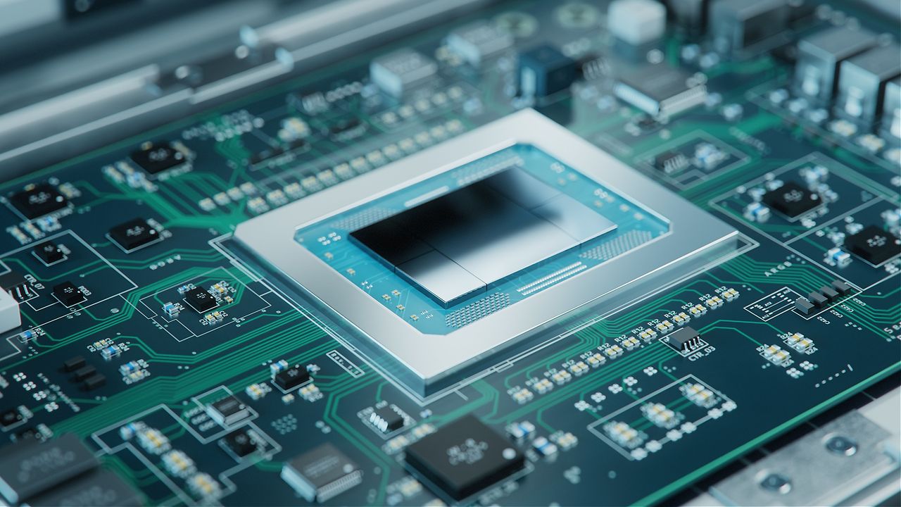


The move toward larger die package architectures — which can be ten times the size of traditional 10-square millimeter packages — has necessitated faster and more efficient application methods. By leveraging capillary motion, modern underfill materials can distribute evenly across complex chip surfaces without external assistance, significantly accelerating production timelines.
Recent industry advancements
New materials are emerging to meet these requirements. For instance, YINCAE has introduced the UF 120LA, a high-purity liquid epoxy underfill. According to Electronicsmedia, this material is engineered for advanced electronics packaging, including BGA, flip chip, and multi-chip modules. A key feature of the UF 120LA is its ability to flow into 20μ gaps, which eliminates the need for intensive cleaning processes during manufacturing.
The performance benchmarks for such materials remain high. The UF 120LA is designed to withstand 5x260°C reflow cycles without suffering from solder joint deformation. As the Chief Technology Officer of YINCAE stated:
"The UF 120LA represents a significant leap forward in electronics packaging technology." “UF 120LA empowers manufacturers to push the boundaries of advanced packaging applications, from BGA to wafer-level chip scale packages. We believe this product will set a new industry standard for performance and efficiency.”
Manufacturing and design implications
The adoption of these materials is not merely about physical protection; it is also about streamlining production workflows. Henkel reports that their latest underfill solutions are 30 percent faster than previous-generation products in mass-production environments. Furthermore, the company has implemented digital modeling approaches to simulate physical testing, which allows customers to evaluate new formulations faster than traditional physical experimentation.
These developments allow for greater customization. Manufacturers can now adjust parameters such as viscosity, curing time, and thermal conductivity to match the unique requirements of specific chip designs. This flexibility is vital for industries such as automotive, 5G infrastructure, and aerospace, where components must function reliably under harsh conditions.
What to watch next
- Next-generation infrastructure: With the introduction of materials capable of supporting 6G infrastructure and autonomous vehicle systems, the focus will shift toward long-term resilience in environments with extreme temperature variations, ranging from minus 65 degrees Celsius to 150 degrees Celsius.
- Integration of AI in design: The use of virtual modeling and automated labs, such as those operated by Henkel in locations like Düsseldorf and Shanghai, will continue to shorten the time-to-market for new semiconductor designs as complexity increases.
As the industry continues to pursue smaller and faster hardware, the role of material science remains the primary bottleneck and the primary enabler of progress. Manufacturers are now looking toward these liquid epoxy advancements to bridge the gap between current production limitations and the performance demands of future data-driven technologies.
How significant is this development?
Contribute your assessment to the aggregated reader intelligence ledger.
Archypedia is dedicated to independent, evidence-backed reporting. This briefing was synthesized from primary source reporting, corroborated across independent newsrooms, and verified against our Editorial Standards.
Transparency record
Evidence behind this report
This report synthesizes 4 distinct sources. Open the source ledger below to compare the underlying coverage.
Prepared under the Archypedia Editorial Policy by the Niko Vale editorial desk profile. AI-assisted tools may support drafting and verification; public accountability remains with Archypedia. Report an error.


